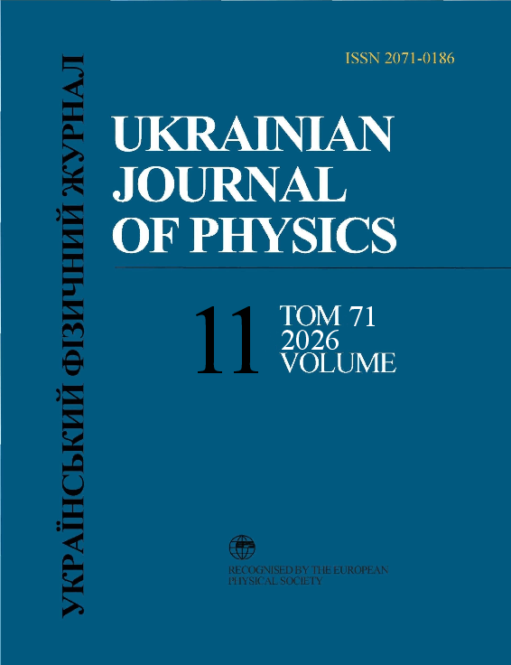
Laser-Induced Crystallization of Ge/Sn Multilayer Amorphous Films
DOI:
https://doi.org/10.15407/ujpe71.11.901Keywords:
GeSn thin films, laser annealing, nanosecond laser, femtosecond laser, XRD, SEM, SIMS, Raman spectroscopy, segregationAbstract
A comparative analysis of the structural, morphological, and optical properties of 150-nm-thick polycrystalline GeSn films formed by laser annealing of amorphous multilayer heterostructures on a Ge/Si(100) buffer layer using two types of radiation – pulsed nanosecond (λ = 355 nm) and femtosecond (λ = 800 nm) was carried out. According to Raman spectroscopy and X-ray diffraction data, pulsed nanosecond UV annealing within a narrow pulse energy density range of 0.2–0.3 J/cm² is most effective for preserving surface planarity and achieving maximum substitutional incorporation of tin (up to 10.3 at.% Sn). Femtosecond annealing provides a lower level of tin incorporation (7.5 at.%) due to intermixing of Sn and Ge elements at the interface between the film and the buffer layer, as confirmed by secondary ion mass spectrometry profiles. It is shown that the surface morphology of the films under these two types of laser processing also differs substantially; in particular, femtosecond annealing causes self-organization of laser-induced periodic surface structures (LIPSS), which are promising for application in specialized optoelectronic devices.
References
1. J.M. Carmona-Sanchez, J. Tiscareno-Ramirez, V. Aca-Aca, A. Hernández-Flores et al. Formation and structural characterization of amorphous GeSn thin films via solid-state Sn diffusion into hydrogenated amorphous germanium. J. Alloys and Compounds 1074, 189195 (2026).
https://doi.org/10.1016/j.jallcom.2026.189195
2. S. Gougam, M.A. Schubert, G. Capellini, M.H. Zoellner. Delayed epitaxial breakdown in MBE-grown GeSn epitaxial layers by high deposition rate and temperatures. J. Phys. D: Appl. Phys. 59, 275106 (2026).
https://doi.org/10.1088/1361-6463/ae83c5
3. A.A. Corley-Wiciak, I. Zaitsev, O. Concepcion, D. Buca et al. Shedding light on epitaxial SiGeSn alloys with Raman spectroscopy: local order and thermomechanical properties. J. Phys.: Condens. Matter. 37, 493002 (2025).
https://doi.org/10.1088/1361-648X/ae1c0b
4. S. Gupta, B. Magyari-Kope, Y. Nishi, K.C. Saraswat. Achieving direct band gap in germanium through integration of Sn alloying and external strain. J. Appl. Phys. 113, 073707 (2013).
https://doi.org/10.1063/1.4792649
5. S. Zaima, O. Nakatsuka, N. Taoka et al. Growth and applications of GeSn-related group-IV semiconductor materials. Sci. Technol. Adv. Mater. 16, 043502 (2015).
https://doi.org/10.1088/1468-6996/16/4/043502
6. R.W. Olesinski, G.J. Abbaschian. The Ge-Sn (Germanium-Tin) system. Bull. Alloy Phase Diagrams 5, 265 (1984).
https://doi.org/10.1007/BF02868550
7. S.V. Kondratenko, Y.V. Hyrka, Y.I. Mazur, A.V. Kuchuk et al. Photovoltage spectroscopy of direct and indirect bandgaps of strained Ge1−xSnx thin films on a Ge/Si (001) substrate. Acta Mater. 171, 40 (2019).
https://doi.org/10.1016/j.actamat.2019.04.004
8. S. Acharya, A. Fischer, N. Rosson, A. Said, H. Stanchu et al. High-quality GeSn grown in foundry mode via chemical vapor deposition enabling lasing up to 235 K. J. Appl. Phys. 138, 173101 (2025).
https://doi.org/10.1063/5.0287945
9. V.O. Yukhymchuk, G.G. Tarasov, M.Ya. Valakh, P.M. Lytvyn et al. Synthesis of Ge1−xSnx and Ge1−x−ySnxCy films by magnetron sputtering followed by laser annealing. Semicond. Phys., Quantum Electron. & Optoelectron. 29 (1), 019 (2026).
https://doi.org/10.15407/spqeo29.01.019
10. V.O. Yukhymchuk, P.M. Lytvyn, A.A. Korchovyi, O.Yo. Gudymenko et al. Laser-induced crystallisation of amorphous GeSn and GeSn:C films. Mater. Res. Express 12, 115004 (2025).
https://doi.org/10.1088/2053-1591/ae1d3d
11. V.O. Yukhymchuk, O.Yo. Gudymenko, T.M. Sabov, O.V. Dubikovskyi et al. Formation and properties of GeSn:C films on silicon substrates. Semicond. Phys., Quantum Electron. & Optoelectron. 27 (4), 412 (2024).
https://doi.org/10.15407/spqeo27.04.412
12. X. Wang, D. Qi, W. Zhou, H. Deng, Yu. Liu et al. Effect of Laser Pulse Width and Intensity Distribution on the Crystallographic Characteristics of GeSn Film. Coatings 13, 453 (2023).
https://doi.org/10.3390/coatings13020453
13. J. Zhang, S. Shangguan, W. Wang, W. Shi et al. Study on the Periodic Structure of Polycrystalline GeSn Prepared by Femtosecond Pulse Laser Direct Writing. SSRN Electronic Journal, http://dx.doi.org/10.2139/ssrn.4402223 (2023).
https://doi.org/10.2139/ssrn.4402223
14. O. Aktas, A.C. Peacock. Laser thermal processing of group IV semiconductors for integrated photonic systems. Adv. Photonics Res. 2, 2000159 (2021).
https://doi.org/10.1002/adpr.202000159
15. J. Bonse. Quo vadis LIPSS? - Recent and future trends on laser-induced periodic surface structures. Nanomaterials 10, 1950 (2020).
https://doi.org/10.3390/nano10101950
16. H. Lin, R. Chen, Yi. Huo et al. Raman study of strained Ge1−xSnx alloys. Appl. Phys. Lett. 98, 261917 (2011).
https://doi.org/10.1063/1.3606384
17. T. Imajo, T. Suemasu, K. Toko. Strain effects on polycrystalline germanium thin films. Sci. Rept. 11, 8333 (2021).
https://doi.org/10.1038/s41598-021-87616-x
18. L.B. Freund, S. Suresh. Thin Film Materials (Cambridge Univ. Press, 2010).
19. Yi. Jie, A.T.S. Wee, C.H.A. Huan, Z.X. Shen, W.K. Choi. Phonon confinement in Ge nanocrystals in silicon oxide matrix. J. Appl. Phys. 109, 033107 (2011).
https://doi.org/10.1063/1.3503444
20. J.I. Langford, A.J.C. Wilson. Scherrer after sixty years: A survey and some new results in the determination of crystallite size. J. Appl. Crystallogr. 11 (2), 102 (1978).
Downloads
Published
Issue
Section
License
Copyright Agreement
License to Publish the Paper
Kyiv, Ukraine
The corresponding author and the co-authors (hereon referred to as the Author(s)) of the paper being submitted to the Ukrainian Journal of Physics (hereon referred to as the Paper) from one side and the Bogolyubov Institute for Theoretical Physics, National Academy of Sciences of Ukraine, represented by its Director (hereon referred to as the Publisher) from the other side have come to the following Agreement:
1. Subject of the Agreement.
The Author(s) grant(s) the Publisher the free non-exclusive right to use the Paper (of scientific, technical, or any other content) according to the terms and conditions defined by this Agreement.
2. The ways of using the Paper.
2.1. The Author(s) grant(s) the Publisher the right to use the Paper as follows.
2.1.1. To publish the Paper in the Ukrainian Journal of Physics (hereon referred to as the Journal) in original language and translated into English (the copy of the Paper approved by the Author(s) and the Publisher and accepted for publication is a constitutive part of this License Agreement).
2.1.2. To edit, adapt, and correct the Paper by approval of the Author(s).
2.1.3. To translate the Paper in the case when the Paper is written in a language different from that adopted in the Journal.
2.2. If the Author(s) has(ve) an intent to use the Paper in any other way, e.g., to publish the translated version of the Paper (except for the case defined by Section 2.1.3 of this Agreement), to post the full Paper or any its part on the web, to publish the Paper in any other editions, to include the Paper or any its part in other collections, anthologies, encyclopaedias, etc., the Author(s) should get a written permission from the Publisher.
3. License territory.
The Author(s) grant(s) the Publisher the right to use the Paper as regulated by sections 2.1.1–2.1.3 of this Agreement on the territory of Ukraine and to distribute the Paper as indispensable part of the Journal on the territory of Ukraine and other countries by means of subscription, sales, and free transfer to a third party.
4. Duration.
4.1. This Agreement is valid starting from the date of signature and acts for the entire period of the existence of the Journal.
5. Loyalty.
5.1. The Author(s) warrant(s) the Publisher that:
– he/she is the true author (co-author) of the Paper;
– copyright on the Paper was not transferred to any other party;
– the Paper has never been published before and will not be published in any other media before it is published by the Publisher (see also section 2.2);
– the Author(s) do(es) not violate any intellectual property right of other parties. If the Paper includes some materials of other parties, except for citations whose length is regulated by the scientific, informational, or critical character of the Paper, the use of such materials is in compliance with the regulations of the international law and the law of Ukraine.
6. Requisites and signatures of the Parties.
Publisher: Bogolyubov Institute for Theoretical Physics, National Academy of Sciences of Ukraine.
Address: Ukraine, Kyiv, Metrolohichna Str. 14-b.
Author: Electronic signature on behalf and with endorsement of all co-authors.